
Latest Research
- 2022.06.22
- Shishido-Kubo Group
Nano-strain analysis of largely bent films towards preventing strain-induced fracture of flexible electronic devices
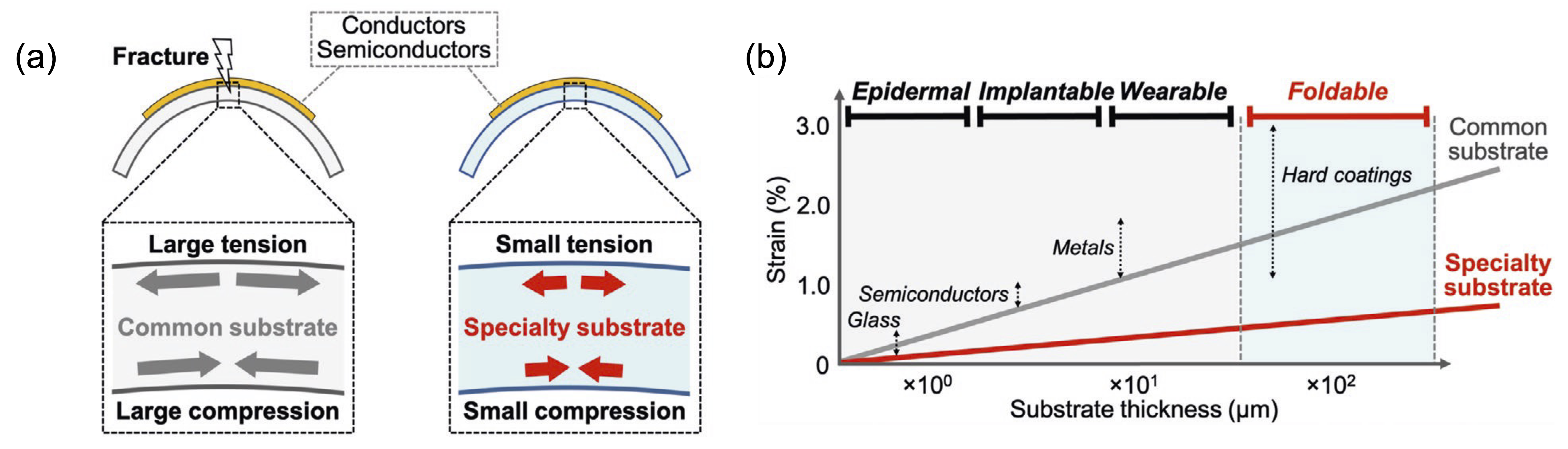
Flexible electronic devices have attracted much attention with the rapid development of flexible electronics and soft robotics. One emerging topic of such devices, at least constructed from flexible substrates, electronic components and coating/sealing layers, is how to prevent fracture of the components integrated on largely bending substrates. Even by deformation at the nanometer scale, strain above the fracture limits inevitably damages any materials, which is the difficulty encountered in developing functional materials for soft robots, biomedical systems, and flexible electronic devices. In flexible electronics, the surface strain of the bending film substrates, exceeding the fracture limits of conductive metals (1-2%), semiconductors (≈1%) and hard coatings (1-3%), causes the failure of the devices as shown in Fig. 1a left.
This difficulty can be circumvented by exploiting an elementary mechanics that surface bending strain decreases linearly with a thickness of a substrate. For example, flexible substrates with a thickness of 10 µm experience peak surface strain of only 0.1% upon bending to the radius of curvature of 5 mm, and this strain remains well below the fracture limits of components. Recently, the use of a substrate within a range below tens of micrometers enables comparable growth, resulting in high-performance durable flexible devices for epidermal, implantable, and wearable applications (Fig. 1b). On the other hand, the development of foldable electronics devices that have thicknesses of hundreds of micrometers is an emerging challenge. This highlights the ever-growing importance of the substrates strategically designed to reduce surface strain without thinning (Fig. 1a right and 1b). However, it is not yet possible to measure nanoscale surface bending strain in real time: none of the currently available advanced methods fulfill all of the necessary spatial-temporal resolution, accuracy, precision, and a wide range of measurable materials.
 |
|
| Fig. 1. | (a) Conceptual illustrations of flexible electronic devices. The common polymeric substrate damages the rigid and brittle electrical materials overlying it through its large surface bending strain that exceeds their fracture limits (left). The specialty substrate with a small surface bending strain that remains below their fracture limits prevents the breakdown of the electrical materials (right). b) Surface strain in a substrate bent with a certain radius of curvature as a function of substrate thickness. Horizontal axis shows the thickness of film substrates integrated into flexible electronic devices for epidermal, implantable, wearable, and next-generation foldable applications. Vertical axis is surface strain, and double arrows show fracture limits of materials such as glass, semiconductors, metals, and hard coatings[1]. |
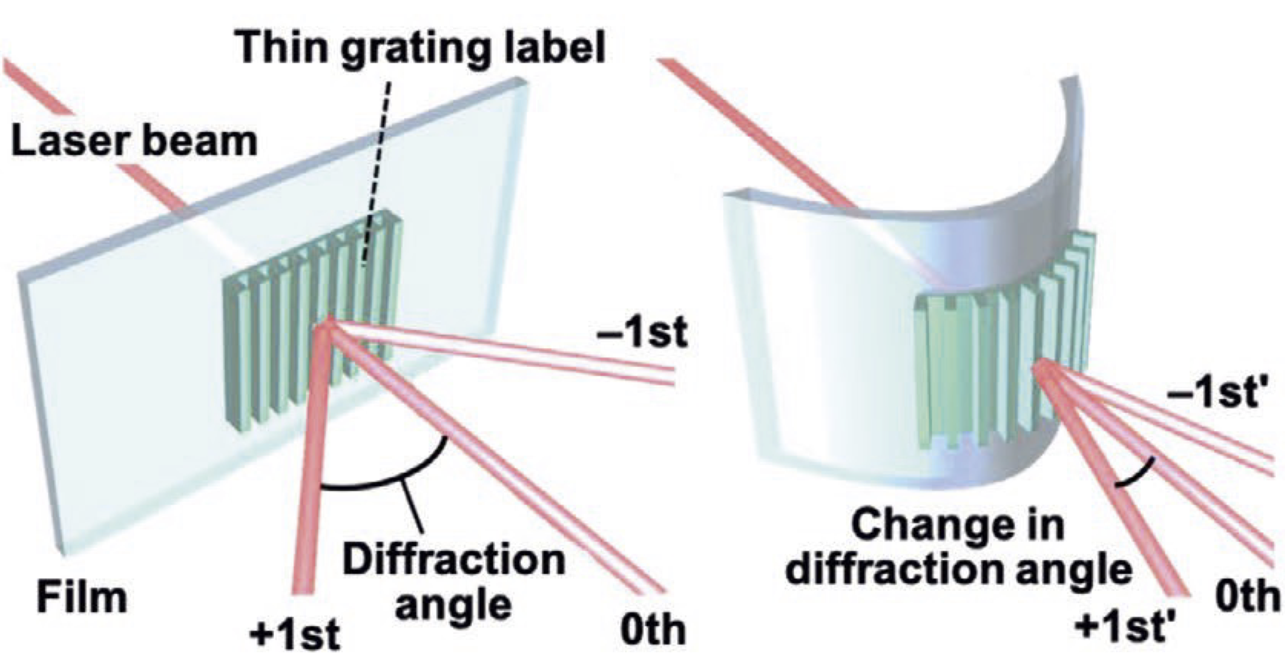
Very recently, we have demonstrated a real-time measurement to quantify a surface bending strain in various flexible film substrates, termed as surface-labeled grating method[1-4]. A soft optical grating label, attached onto surface of target materials, can diffract an incident probe beam with a diffraction angle depending on the grating period. Under bending deformation of target materials, the surface strain and diffraction angle change. This allows us to quantitatively analyze the surface bending strain with high accuracy and precision in a single nanometer scale (<1.0 nm and <0.01% strain). Besides, the real-time strain analysis method has an advanced benefit: a wide range of measurable materials with surface flatness. We have confirmed that the surface bending strain of multilayered films, composed of flexible polymeric substrates, glasses, metals, and/or semiconductors, can be quantitatively measured.
 |
|
| Fig. 2. | Schematic of underlying principle of surface bending strain analysis using a soft, thin grating label, termed surface-labeled grating method. The film with the grating label diffracts the incident laser beam with a diffraction angle depending on the grating period (left). When the film bend, the surface strain increases, leading to changes of the grating period and diffraction angle (right)[1]. |
As a proof-of-concept experiment for preventing fracture of flexible electronic devices, we first evaluated a surface bending strain of a hard coatings that is often used as a protection layer for current devices such as smartphones. We revealed that the cracking of hard coatings on the surface of PET films occurred at surface strains exceeding 1.45%, regardless of the film thickness and curvature. On the basis of this experimental value of the fracture limit, we designed the triple-layered system where a soft silicone elastomer layer is sandwiched with two PET layers. This enables to reduce the surface bending strain by 60% compared with that of a single-layer film with the same thickness, thereby achieving the surface bending strain of below 1.0% at the radius of curvature of 4 mm. This triple-layer film successfully suppressed the cracking of the hard coating. Furthermore, with a cooperation of Prof. Takeya from The University of Tokyo, an organic transistor was fabricated on our designed triple-layered substrate. This substrate design reduced the surface bending strain and successfully suppressed the breakdown of the organic transistor without degradation of device performance.
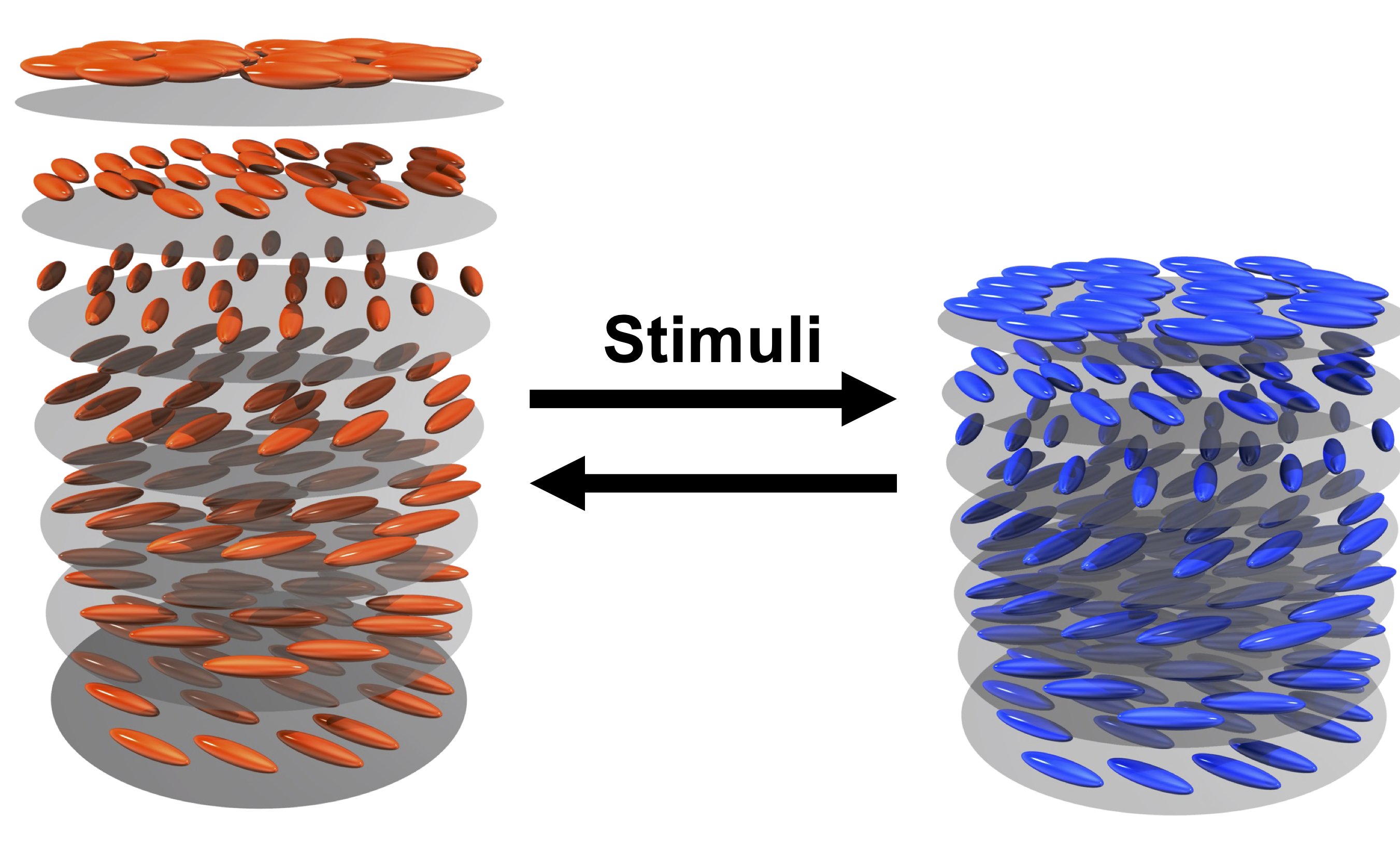
Besides developing surface-labeled grating method, our group are engaging in a variety of research projects to establish the dynamics of flexible devices though quantitative analysis of deformation behavior. Our collaboration with Prof. Tsutsumi from Ritsumeikan University, under the Cooperative Research Program of "Network Joint Research Centre for Materials and Devices (Tokyo Institute of Technology)", has led to the development of a simple but powerful method for analyzing strain by means of cholesteric liquid crystals[5,6]. A cholesteric liquid crystal possesses an intrinsic nanostructure of helically twisted molecular orientation, showing bright reflection color. The nanostructure and reflection color changes under external stimuli such as mechanical force, allowing us to analyze deformation behavior of target materials by using the change of reflection color (Fig. 3).
 |
|
| Fig. 3. | Schematics of the molecular orientation of a cholesteric liquid crystal without (left) and under (right) an applied external stimulus. The cholesteric liquid crystals possess periodic nanostructure of helically twisted molecular orientation, showing reflection color. The reflection color depends on the periodicity and changes under an applied external stimulus. The ellipsoids show the liquid crystal directors. |
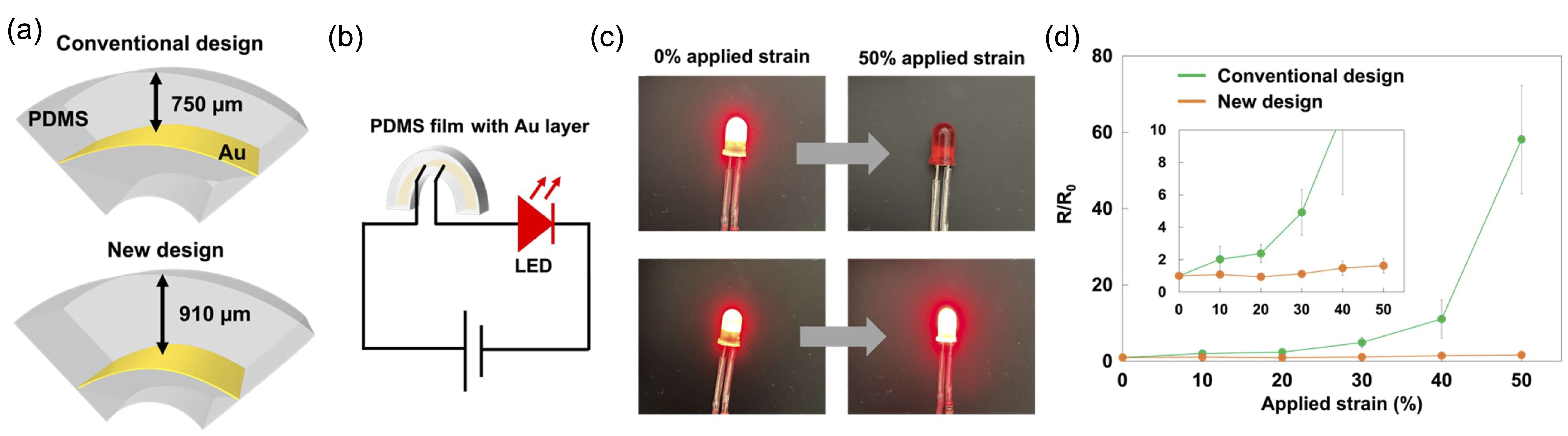
Flexible electronic devices composed of multiple layers, such as soft polymers/elastomers, metals, and semiconductors, might cause fracture of internal layers, leading to degradation of their performance under bending deformation. To directly identify the strain distribution in an internal layer, we have employed cholesteric liquid crystals, which acts as a strain visualizer without any external electrical connections. The cholesteric liquid crystal film, located at an internal layer of a multilayered material, enabled to visualize the positional shift of neutral mechanical plane (NMP) in which the strain becomes zero inside bending materials. This is the first report on identification of the NMP position, revealing that bending of the soft silicone film reversibly shifts the NMP position (Fig. 4)[6]. Based on the NMP shifting, we designed the structure of a flexible electronic device with an Au layer deposited near the NMP and succeeded to suppress the increase of electrical resistance due to fracture of the Au layer compared with those with conventional structure. Experimental identification of the NMP position in bending soft materials will aid in the structural design of flexible electronic devices with high mechanical durability.
 |
|
| Fig. 4. | (a) Illustrations of the fabricated devices based on the conventional design containing the Au layer at a depth of 750 μm (upper) and the new design, containing the Au layer at a depth of 910 μm considering the NMP shift (lower). (b) Schematic of the circuit layout. (c) The LED is connected to the Au layer in the PDMS films. Photographs of LEDs of the conventionally (upper) and newly designed devices (upper) at 0% (left) and 50% applied strain (right). (d) Electrical resistance of the conventionally and newly designed devices as a function of applied strain. Each point represents the average of three samples. The error bars denote standard deviation[6]. |
In modern era, the development of flexible/wearable electronic devices such as bendable smartphones are moving forward rapidly. We believe that the realization of practical deformation analysis tools, such as the surface-labeled grating method, enables to provide design strategy of flexible materials with desired performance and contributes to boosting the exploration of efficient fabrication route of next-generation devices in the field of not only electronics but also soft robotics.
References
| [1] | R. Taguchi, N. Akamatsu, K. Kuwahara, K. Tokumitsu, Y. Kobayashi, M. Kishino, K. Yaegashi, J. Takeya, A. Shishido, Adv. Mater. Interfaces, 8, 2001662 (2021). |
| [2] | 宍戸 厚,コンバーテック, 加工技術研究会, 49, 64-66 (2021). |
| [3] | K. Kuwahara, R. Taguchi, M. Kishino, N. Akamatsu, K. Tokumitsu, A. Shishido, Appl. Phys. Express, 13, 056502 (2020). |
| [4] | 田口 諒・赤松 範久・宍戸 厚, 次世代ディスプレイへの応用に向けた材料、プロセス技術の開発動向, 技術情報協会, 118-128 (2020). |
| [5] | K. Hisano, S. Kimura, K. Ku, T. Shigeyama, N. Akamatsu, A. Shishido, O. Tsutsumi, Adv. Funct. Mater., 31, 2104702 (2021). |
| [6] | M. Kishino, N. Akamatsu, R. Taguchi, K. Hisano, K. Kuwahara, O. Tsutsumi, J. Takeya, A. Shishido, Adv. Eng. Mater., in press. DOI: 10.1002/adem.202101041. |